Anatomy Of Switching Power Supplies
페이지 정보

본문
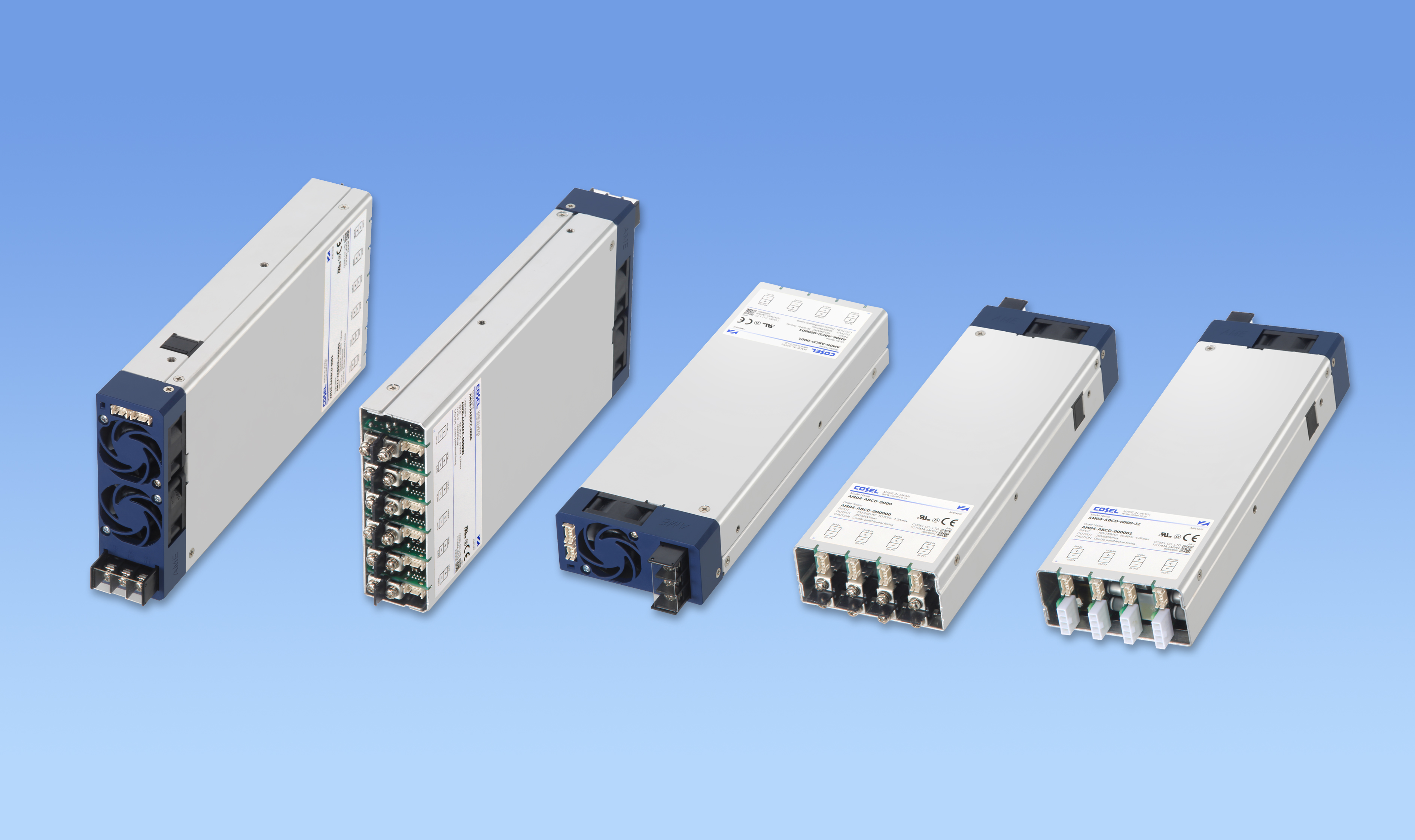
Typically as an alternative of a transformer an optocoupler (a small integrated circuit containing a LED and a phototransistor packed collectively) is used. As we mentioned, the PWM control circuit makes use of the ability provide outputs to manage how it's going to drive the switching transistors. If the output voltage is flawed, the PWM control circuit adjustments the waveform applied on the switching transistors as a way to appropriate the output. On the subsequent pages we're going to discover every one of these stages with photos showing where you could find them inside a energy supply. After opening a power provide for the very first time (don’t do this with its power cord attached or you will get an electrical shock), you could find yourself fairly misplaced making an attempt to determine what's what. But you will recognize at the least two belongings you already know: the ability supply fan and some heatsinks.
Electronic components are used for Renewable vitality applications, Power electronics, and Biomechanics. Electronic components are utilized in Aerospace & Defense and Medical Devices like Advanced units are being carried out for recording the data. We've got learnt about the electronic components ,and we now have seen the classification of electronic components, These resistance, inductance, and capacitance are called passive circuit electronic components and they don't switch electrical power. 1. The transducers listed listed here are single electronic components (as opposed to complete assemblies), and are passive (see Semiconductors and コーセル Tubes for active ones). Solely the most typical ones are listed right here. On a circuit diagram, electronic units are represented by typical symbols. Reference designators are utilized to the symbols to establish the parts.
Though the construction is very different from the bipolar transistor, what goes on may be very related. The P and N junction types a depletion area as before, so no cost carriers can be found to conduct. Therefore, the drain (D) and source (S) have a high resistance between them. Area impact transistors break down the depletion layer by making use of a positive voltage to the gate (G), allowing the current to movement between the drain and supply (red arrow within the diagram above). Metal Oxide Field Effect Transistors, or MOSFETs, have a skinny metal oxide insulating layer separating the gate from the P-type materials. The kind is decided by the atomic structure of the precise semiconductor material. Now, consider an npn transistor. Every finish of the transistor is an n-kind semiconductor material and between them is a p-kind semiconductor material. By varying the potential in each region, then, you may drastically have an effect on the rate of electron circulation throughout the transistor.
- 이전글The Reason Replacement Windows Is Fast Becoming The Hottest Trend Of 2023 24.04.09
- 다음글Mobile Auto Diagnostic Services Near Me: The Secret Life Of Mobile Auto Diagnostic Services Near Me 24.04.09
댓글목록
등록된 댓글이 없습니다.